Particles and nanostructure
Compare particle size, shape, dispersion, agglomeration and internal contrast at nanometre scale.
Material Analysis · Microscopy & Imaging
See internal nanoscale structure, particle morphology, lattice features, defects and interfaces in electron-transparent specimens, with optional diffraction and local chemical analysis.

Why this test
TEM transmits electrons through an ultra-thin region; STEM scans a focused probe across it. Together they connect nanoscale morphology, crystallography and local chemistry to the same feature.
Compare particle size, shape, dispersion, agglomeration and internal contrast at nanometre scale.
Use HRTEM, FFT or lattice-spacing measurements and SAED to investigate local crystal information.
Examine grain boundaries, dislocations, stacking faults, coatings, multilayers and buried interfaces.
Add STEM-EDS or EELS when elemental distribution or electronic and chemical information is central.
Choose grid preparation, ion milling, FIB lift-out or ultramicrotomy around the target region and material.
Choose the scope
The target feature, required spatial resolution, elements of interest and preparation route determine the most useful acquisition mode.
Best for nanoparticle morphology, size, dispersion, agglomeration and internal contrast.
Best for lattice fringes, crystallinity, orientation and local phase evidence.
Best for Z-contrast imaging, interfaces and scanning acquisition correlated with spectroscopy.
Best for local elemental distribution and selected electronic or chemical-state questions.
Common outputs
Fields of view, modes, measurements, file formats and raw-data availability are agreed before preparation and acquisition.
TEM / STEM image set supplied with the agreed units, labels, sample reference and measurement conditions.
Acquisition context supplied with the agreed units, labels, sample reference and measurement conditions.
HRTEM and lattice evidence supplied with the agreed units, labels, sample reference and measurement conditions.
SAED patterns supplied with the agreed units, labels, sample reference and measurement conditions.
EDS analysis supplied with the agreed units, labels, sample reference and measurement conditions.
EELS and native files supplied with the agreed units, labels, sample reference and measurement conditions.
Specialist modes: aberration-corrected TEM/STEM, in-situ holders, 4D-STEM, tomography, Lorentz TEM and cryogenic workflows require a separate feasibility and quotation review.
Illustrative examples
These simulated examples explain the output types only. Customer results depend on the specimen, preparation route and agreed acquisition conditions.
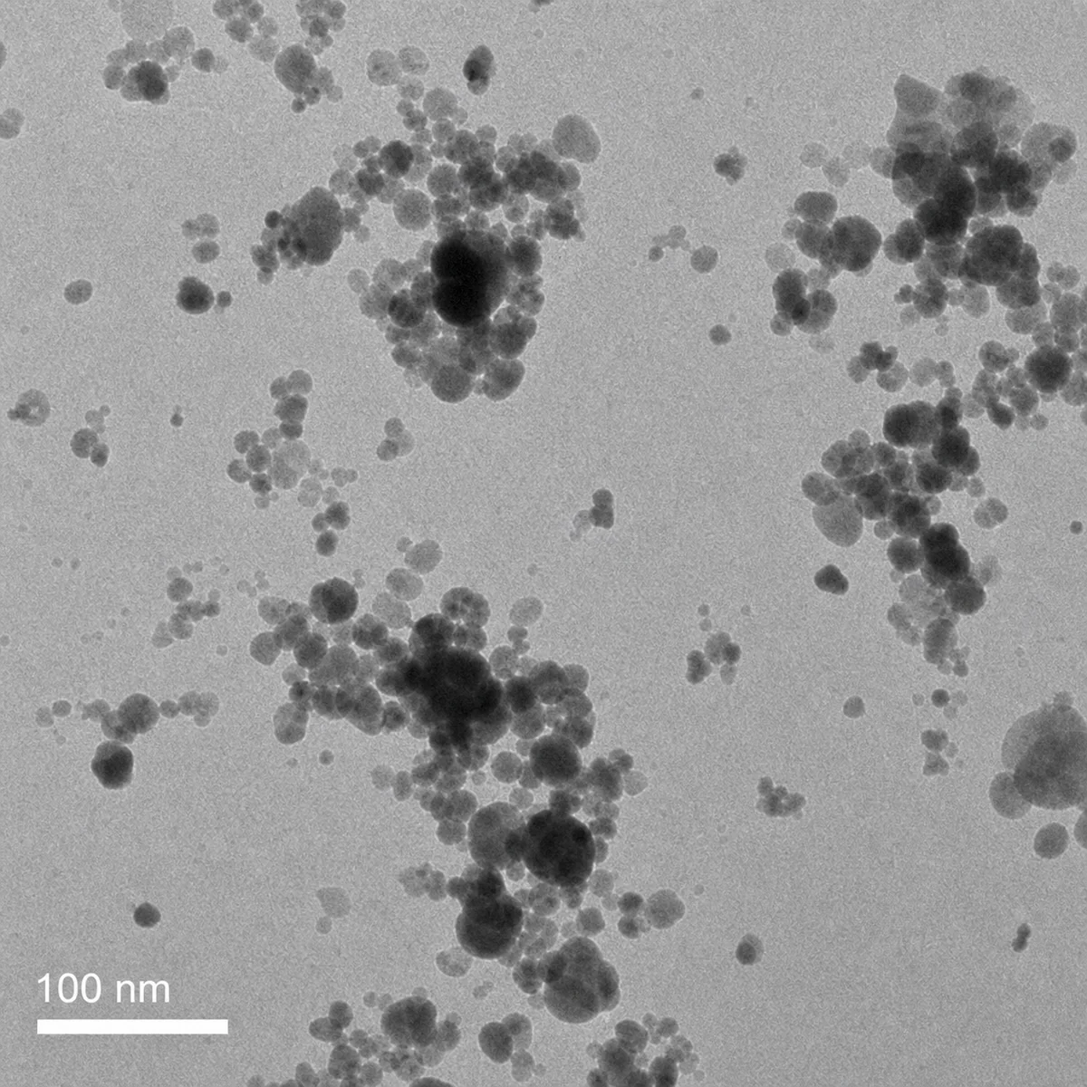
Overview and detail images can show particle size, shape, agglomeration and local contrast.
Illustrative simulated output, not customer data.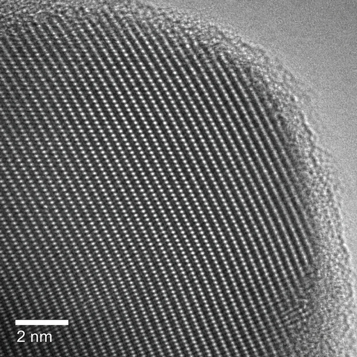
High-resolution images can support lattice-spacing and interface interpretation where specimen quality permits.
Illustrative simulated output, not customer data.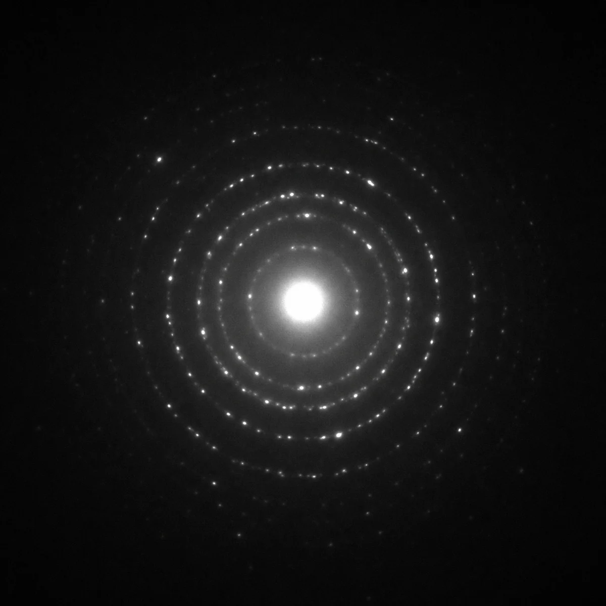
Selected-area diffraction can support phase, orientation and crystallinity assessment.
Illustrative simulated output, not customer data.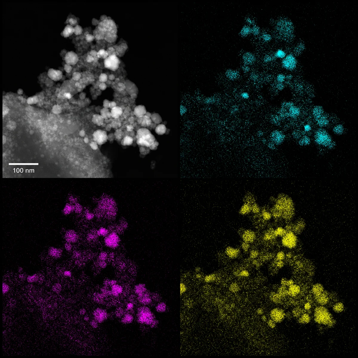
Correlated HAADF-STEM and EDS views can compare structure with local elemental distribution.
Illustrative simulated output, not customer data.Sample requirements
The target region must be electron-transparent, clean and stable enough for the requested imaging or spectroscopy mode.
| Sample type | Preferred submission | Preparation and information required |
|---|---|---|
| Powders and nanoparticles | Small representative quantity | State composition, expected size, dispersion solvent and whether carbon, copper or another grid material must be avoided. |
| Stable dispersions | Practical volume confirmed after review | Provide solvent, concentration, dispersant or surfactant and stability information. Confirm whether dilution is acceptable. |
| Thin films and membranes | Electron-transparent area or preparation stock | Mark plan-view or cross-section orientation and identify the target layer, interface or feature. |
| Bulk and cross-sections | Preparation stock sized to the agreed route | Usually require FIB lift-out, ion milling, twin-jet electropolishing or ultramicrotomy. Mark the exact target location. |
| Prepared grids or lamellae | Protected and clearly labelled | Identify grid or lamella, orientation, priority regions and previous preparation or coating steps. |
| Special-handling samples | Advance review required | Declare magnetic, volatile, vacuum-unstable, air/moisture-sensitive, beam-sensitive, toxic, biological or radioactive properties before shipment. |
Grid selection: tell us when carbon, copper, nickel, molybdenum or another support could interfere with the intended analysis.
Region of interest: include a marked image, drawing or coordinate reference for site-specific interfaces, coatings, defects or particles.
Questions and answers
Short answers to the issues that most often change preparation, platform or interpretation.
TEM forms an image from electrons transmitted through a thin specimen. STEM scans a focused probe and records signals point by point, which is especially useful for HAADF contrast and correlated elemental mapping.
Not always. Nanopowders and stable dispersions can often be deposited directly onto grids. Bulk materials, coatings, interfaces and site-specific cross-sections commonly need FIB or another thinning route.
HRTEM and diffraction can provide local lattice and crystallographic evidence. Reliable phase identification may also need calibration, indexing and complementary XRD or spectroscopy.
Often, but feasibility depends on thickness, stability, element sensitivity, signal level, spatial resolution and the available detector configuration. State the target elements or edges before quotation.
Only a small quantity may be consumed, but the practical amount depends on concentration, preparation route and repeat work. We confirm submission quantity after reviewing the sample.
Excess thickness, contamination, unstable dispersion, beam damage, charging, drift, strong magnetism, poor target definition and preparation artefacts can all limit the result.
Request a quote
A £45 service fee applies to orders under £300, excluding VAT.
Typical turnaround: 8–12 working days
Configure & Book